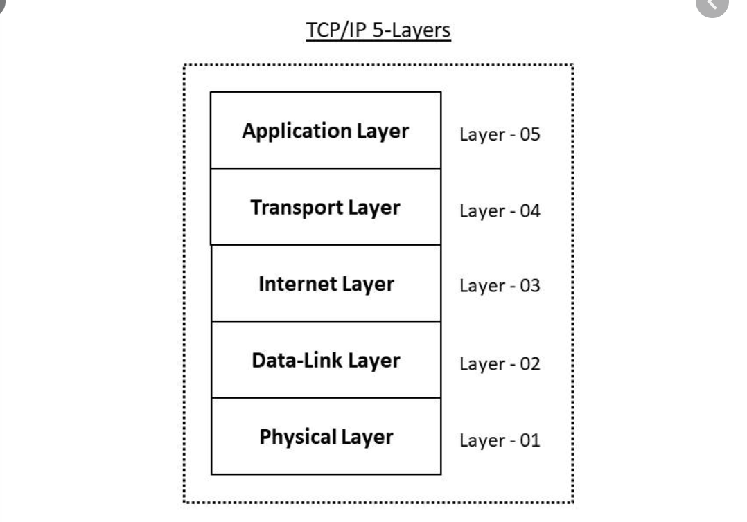
A reference of the 5 layer networking model (analogy purposes)
A reference of the 5 layer networking model (analogy purposes)
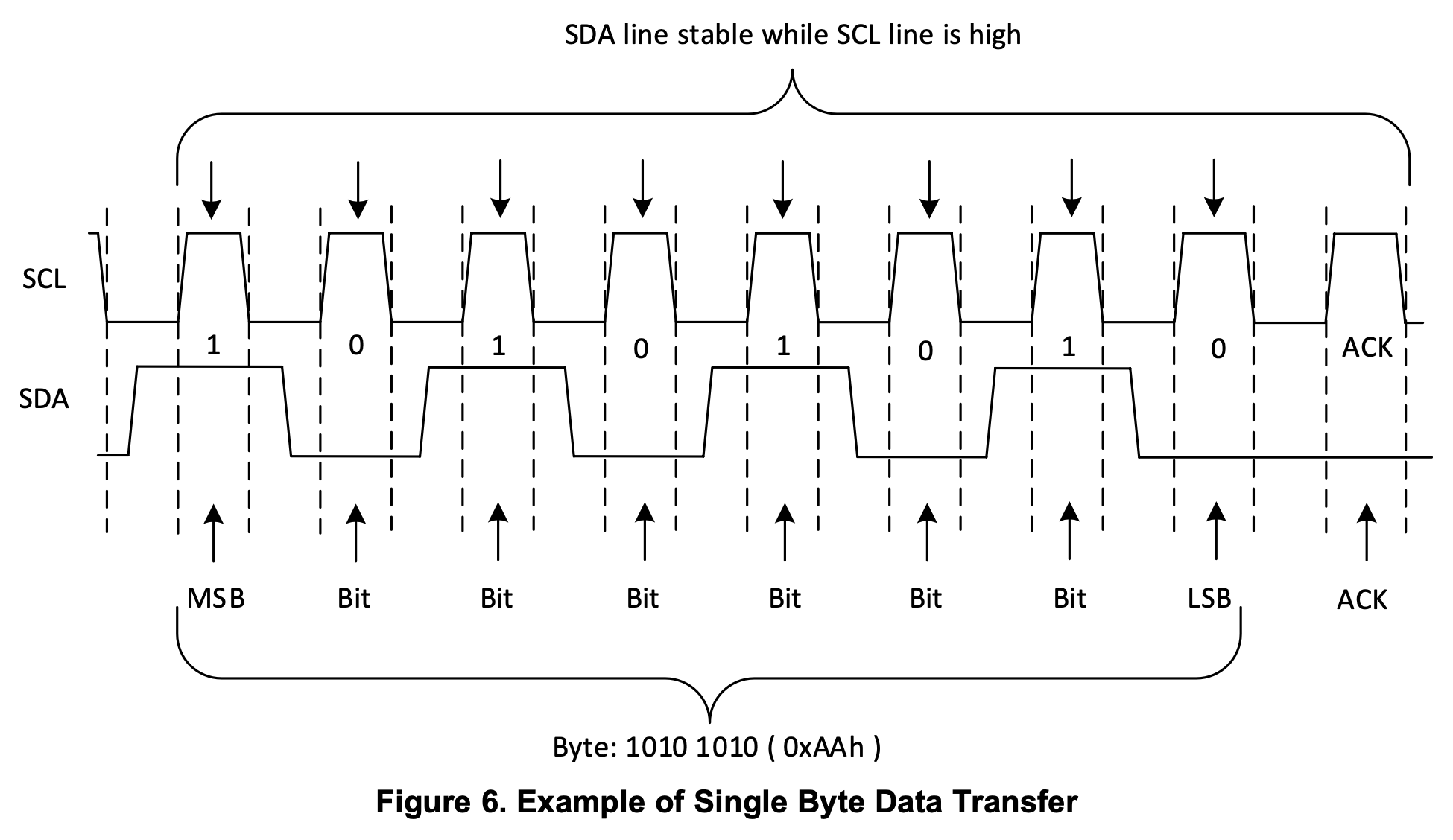
From TI I2C documentation, pg. 4
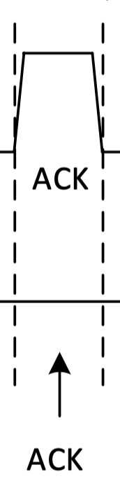
Example of an ACK
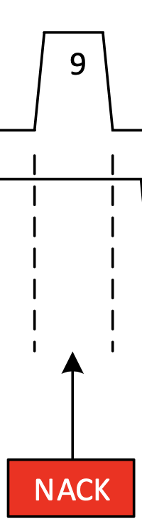
Example of NACK
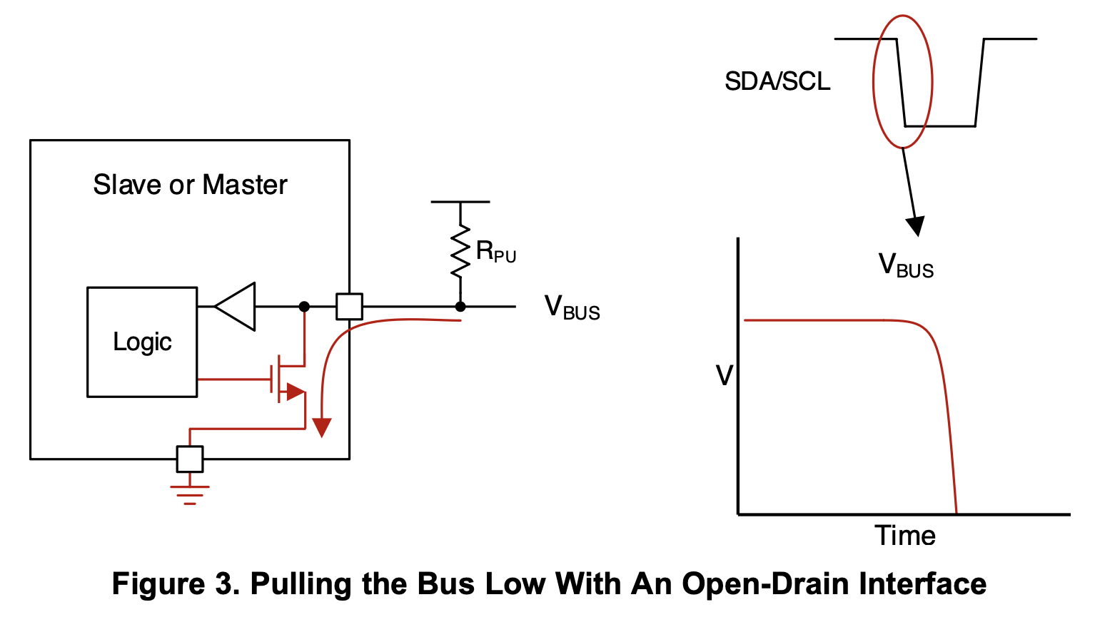
From TI I2C documentation, pg. 4
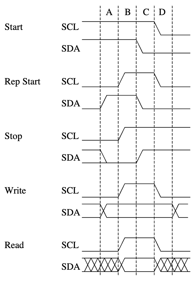
From OpenCores reference, pg. 15
Each operation split into ⅘ signal level operations
FSM flow chart